PCB data management
How to organize PCB project files so manufacturing does not use the wrong revision.
If your PCB files live in random folders named final, final-new, sent-to-fab, client-latest, and old-dont-use, you do not have a file system. You have a future production mistake waiting quietly.
Direct answer: the simplest PCB project structure
Use one root folder per product or client project. Inside it, separate working design files from frozen release packages. A practical structure is: `01_design`, `02_datasheets`, `03_bom`, `04_firmware`, `05_manufacturing_releases`, `06_test_and_debug`, `07_images`, and `99_archive`. Every manufacturing release should have its own folder with Gerbers, drills, BOM, pick-and-place, assembly notes, test instructions, and a release note.
Recommended PCB project folder structure
The exact folder names matter less than the discipline behind them. The key rule is simple: editable files and released files should not live in the same pile.
Product-Name-or-Client-Project/
  00_admin/
  01_design/
    schematic/
    pcb_layout/
    exports_for_review/
  02_datasheets/
  03_bom/
  04_firmware/
  05_manufacturing_releases/
    HW-R1_prototype_2026-06-06/
    HW-R2_pilot_2026-07-15/
  06_test_and_debug/
  07_images_and_renders/
  99_archive/
This makes it obvious where current work happens and where released packages live. If someone needs files for fabrication, they should go to `05_manufacturing_releases`, not dig through CAD exports.
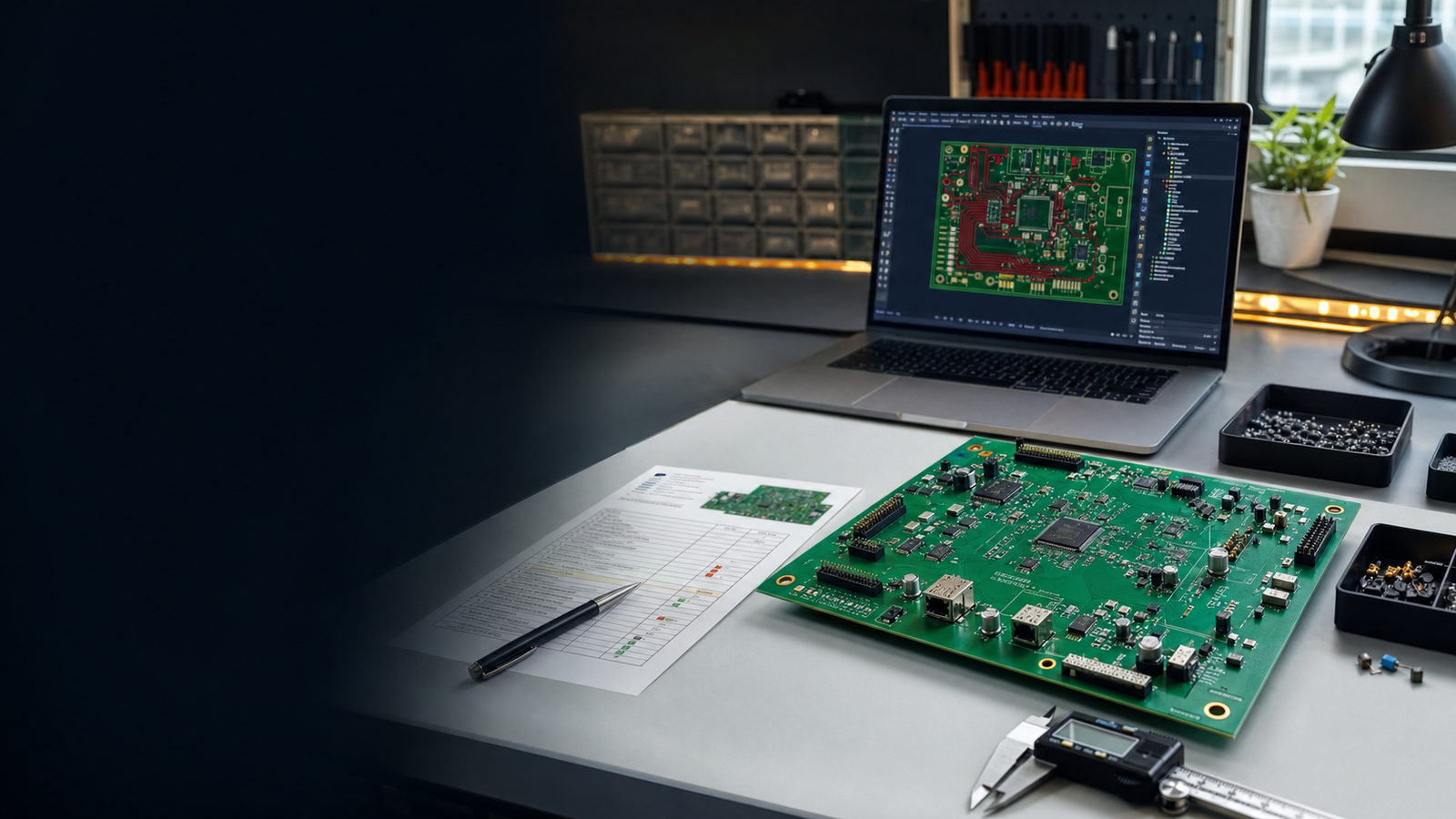
What to include in a PCB manufacturing release package
A release package is the file set you are comfortable sending to a PCB fabricator, assembly vendor, client, or internal production team. It should be frozen and traceable.
| File | Why it matters | Common mistake |
|---|---|---|
| Gerber zip | Defines copper, solder mask, silkscreen, paste, and board outline layers. | Sending Gerbers exported before the last connector or footprint change. |
| Drill files | Defines plated and non-plated holes for vias, connectors, and mounting. | Forgetting drill files or mixing drill files from another revision. |
| BOM | Defines components, quantities, values, footprints, MPNs, and alternates. | Purchase uses a different BOM from the one assembly uses. |
| Pick-and-place | Needed for SMT assembly orientation and placement. | Coordinates exported from an old layout or not matching the BOM. |
| Assembly notes | Explains polarity, DNP parts, jumpers, hand-soldered items, and special handling. | Assuming the assembler knows the intent hidden inside the schematic. |
| Test instructions | Defines first power-up checks, voltage rails, firmware load, and pass/fail criteria. | No one knows how to verify the first assembled board. |
| Release note | Records revision, date, change reason, known risks, and who approved it. | Months later, nobody remembers why this board exists. |
Naming rules for PCB revisions
Avoid emotional filenames like `final`, `latest`, `new`, or `use-this-one`. Use revision names that survive tired teams, vendor confusion, and six-month-old support calls.
- Use hardware revision names such as `HW-R1`, `HW-R2`, or `HW-R3`.
- Add release purpose: `prototype`, `pilot`, `production`, or `field-fix`.
- Add date in ISO format: `2026-06-06`, not `6-6-26`.
- Use the same revision name across Gerber, BOM, firmware, drawings, and test notes.
- Never overwrite a release package after sending it out. Create a new release.
`HW-R2_pilot-release_2026-07-15` is much clearer than `final_new_client_sent`.
Do not separate BOM and firmware from the PCB revision
Electronics products often fail because the PCB, BOM, and firmware are treated like separate worlds. A connector pin changes, a pullup value changes, a module changes, or an I2C address changes, and suddenly firmware written for one revision behaves badly on another.
If a regulator, oscillator, connector, sensor, or transistor is substituted, record which hardware revision accepts it.
Store firmware version, pin mapping, bootloader notes, and configuration files with the PCB revision they support.
First article test notes should say which release package and firmware build were tested.
Common PCB file organization mistakes
| Mistake | Better system |
|---|---|
| Keeping Gerbers in the same folder as editable design exports. | Put frozen manufacturing files inside a dedicated release folder. |
| Sending files from WhatsApp, email, and Drive without a single source of truth. | Use one release package link or folder for each manufacturing batch. |
| Using `latest` or `final` in filenames. | Use revision, purpose, and date. |
| Not storing datasheets and supplier notes. | Keep datasheets, alternates, and sourcing decisions beside the BOM. |
| Not recording what was actually sent to the PCB manufacturer. | Freeze the exact sent package and record the vendor/date/batch. |
When folders are no longer enough
Folders work for one person and a few projects. They start breaking when you have clients, team members, purchase people, assembly vendors, firmware versions, field failures, or repeated manufacturing batches.
PCB Vault Software is being built for this exact problem.
It is the front-door software product for organizing PCB projects, Gerbers, BOMs, schematics, revisions, manufacturing release packages, and handoff notes in one place.
FAQ
What is the best folder structure for PCB projects?
Use one project root with folders for design, datasheets, BOM, firmware, manufacturing releases, test/debug notes, images, and archive. Keep releases separate from editable work.
Should I zip every PCB release?
Yes, for handoff. Keep the source release folder, but create a zip that contains the exact files sent to the manufacturer or client.
Should BOM files have revision numbers?
Yes. The BOM should clearly match the hardware revision and release package. A BOM without revision context is dangerous in production.
Can Git solve PCB file organization?
Git can help technical teams with source history, but it does not automatically create manufacturing release packages, BOM approvals, vendor handoff notes, or purchasing context.