Complete PCB design tutorial
PCB design tutorial for beginners to advanced: tools, calculations, layout rules, Gerbers, BOMs, and release files.
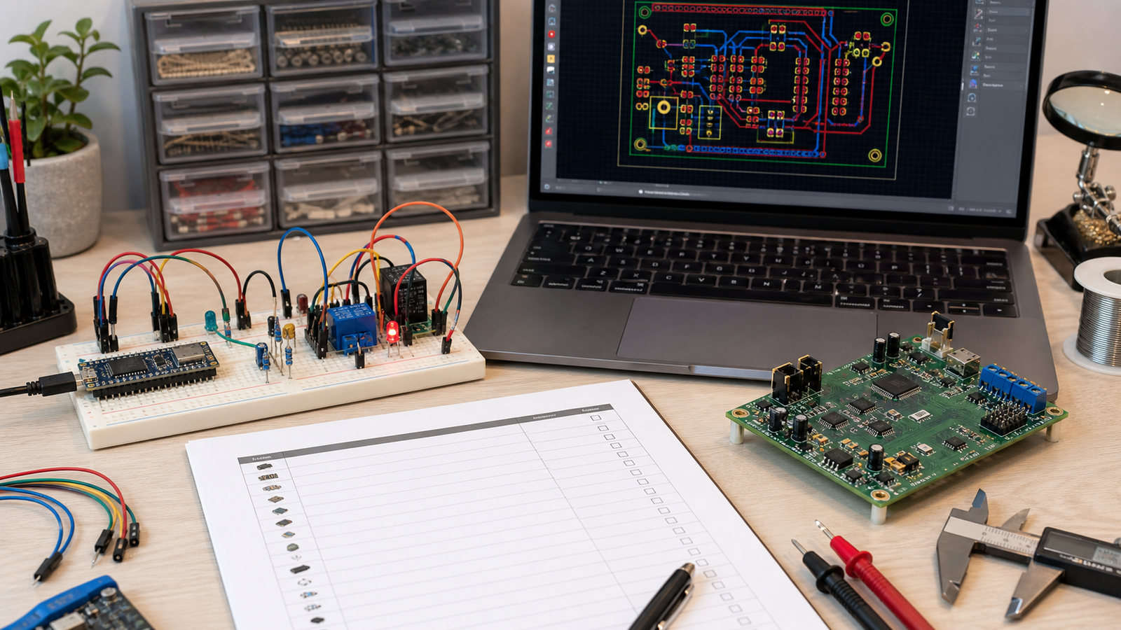
This is the complete PCB design path: start with electronics and schematic basics, learn layout and routing rules, understand the calculations that affect real boards, prepare manufacturing files, and build a release system so the correct PCB revision reaches fabrication.
Quick answer: the complete PCB design workflow
Define the product requirements, prove the circuit, draw the schematic, assign real footprints, choose stack-up and design rules, place parts intentionally, route power and signals, run ERC/DRC/DFM checks, inspect Gerbers, create BOM and assembly outputs, then freeze a release package with revision notes. Beginners can start with simple 2-layer boards. Advanced designers add impedance control, EMI planning, thermal design, high-speed constraints, panelization, test strategy, ECO control, and release traceability.
PCB design learning roadmap: beginner to advanced
| Level | What to learn | What you should be able to build |
|---|---|---|
| Beginner | Schematic, footprints, 2-layer layout, DRC, Gerber export | LED board, sensor board, Arduino/ESP32 carrier, simple regulator board |
| Intermediate | Power paths, ground planes, connectors, BOM, assembly files, DFM | Reliable prototype with connectors, mounting, test points, and manufacturing notes |
| Advanced | Impedance, high-speed routing, EMI, thermal, stack-up, panelization, ECOs | Production-ready electronics with controlled releases and supplier handoff |
PCB design tools you should know
CAD tools
KiCad is the best default recommendation for beginners because it is free, powerful, and exports standard manufacturing files. EasyEDA is easier for quick boards and JLCPCB workflows. Altium Designer is common in professional teams. Fusion/EAGLE appears in maker and mechanical workflows.
Verification tools
Use ERC for schematic checks, DRC for layout rule checks, a Gerber viewer for manufacturing output, a 3D viewer for mechanical conflicts, and a BOM checker for part availability and package matching.
PCBVault workflow tools
Use a project folder template, versioned release folders, BOM revision tracking, and PCBVault Software when the project has multiple revisions, clients, teammates, or manufacturing handoffs.
PCB terminology beginners must understand
| Term | Meaning | Why it matters |
|---|---|---|
| Schematic | Logical circuit diagram | Defines how components connect electrically |
| Footprint | Physical pad pattern on PCB | Wrong footprint can make the board unusable |
| Net | Electrical connection name | Guides layout and design checks |
| Trace | Copper route between pads | Width and length affect current, loss, and noise |
| Via | Plated hole connecting layers | Needed for routing but adds impedance and manufacturing constraints |
| Plane | Large copper area for ground or power | Improves return paths, noise, and current distribution |
| Gerber | Fabrication layer file | Used by PCB manufacturers to build the board |
| BOM | Bill of materials | Defines exactly which parts are assembled |
| Pick-and-place | Component location file | Used for automated assembly |
| DRC | Design rule check | Catches clearance, width, and unconnected errors |
Step 1: define requirements before drawing
Write down the board purpose, power input, maximum current, connectors, mounting holes, enclosure limits, expected temperature, communication interfaces, programming method, test method, and manufacturing plan. This prevents random layout decisions later.
- Input voltage range and reverse-polarity protection.
- Maximum current for every rail and high-current load.
- Connector orientation, pinout, cable direction, and strain relief.
- Board size, mounting holes, keepouts, and enclosure constraints.
- Assembly method: hand soldering, stencil, reflow, or vendor assembly.
Step 2: schematic design best practices
Use meaningful net names, power symbols, connector labels, decoupling capacitors, pullups, programming headers, test points, and notes. Run ERC before layout. If the schematic is unclear, the PCB will inherit that confusion.
Schematic checklist
- Use consistent symbols and readable signal flow from left to right.
- Name power rails clearly: `VIN`, `5V`, `3V3`, `VBAT`, `GND`.
- Add decoupling capacitors near every IC power pin.
- Show connector pin numbers and polarity.
- Add test points for power, reset, programming, and important buses.
Step 3: footprint selection and library control
Every schematic symbol must match the real package you will buy. Check pad pitch, pin numbering, polarity, body size, courtyard, height, and assembly orientation. A correct schematic with a wrong footprint still creates a bad board.
Step 4: layers, stack-up, and material choices
Most beginner boards can start with 2 layers: top copper, bottom copper, solder mask, and silkscreen. Use 4 layers when you need stronger ground return, denser routing, reduced EMI, controlled impedance, or cleaner power distribution.
| Board type | Use when | Watch out for |
|---|---|---|
| 2-layer | Low-speed sensors, microcontrollers, simple power | Ground return can be messy if routing is careless |
| 4-layer | WiFi, USB, dense layouts, lower noise, better EMC | Higher cost and stack-up choices matter more |
| 6+ layer | High-speed digital, DDR, complex RF, dense products | Requires impedance, via, and fabrication planning |
Important PCB calculations
Trace width and current
Trace width depends on current, copper thickness, allowed temperature rise, and whether the trace is external or internal. For beginner boards, use a trace width calculator and add margin. Do not route motor, relay, heater, LED strip, or GSM current through thin signal traces.
Voltage drop
Long thin traces drop voltage. If a module resets when a load turns on, calculate voltage drop across the path and connector. Keep high-current paths short and wide.
Power dissipation and thermal rise
Linear regulators, MOSFETs, current shunts, and protection diodes can heat up. Estimate power with `P = V x I` or `P = I^2 x R`, then plan copper area, thermal vias, or a different part.
Pullup and pulldown resistors
I2C pullups, boot pins, reset pins, and enable pins need correct resistor values. Too weak can be noisy. Too strong can waste current or fight another device.
Impedance basics
Controlled impedance matters for high-speed USB, Ethernet, RF, fast clocks, and differential pairs. Beginners do not need to calculate every trace, but should know when a signal is no longer "just a wire."
Component placement guidelines
Good placement makes routing easier. Bad placement makes routing impossible. Place connectors first, then mechanical parts, then power blocks, then ICs, then passives. Keep decoupling capacitors close to IC pins. Keep crystals close to MCU pins. Keep hot or noisy sections away from sensors and analog inputs.
- Put connectors on board edges unless there is a mechanical reason not to.
- Keep high-current loops physically small.
- Group parts by function: power, MCU, sensors, communication, output drivers.
- Leave access for probes, screws, cables, and assembly tools.
PCB routing best practices
Route power first, then critical signals, then slower signals. Use wider traces for current. Keep traces short where noise, timing, or impedance matter. Avoid routing sensitive analog signals near switching regulators, motors, relays, antennas, or high-current loops.
Beginner routing rules
- Use manufacturer minimums only when necessary; wider clearance is safer.
- Avoid unnecessary layer changes and via chains.
- Use 45-degree bends or smooth routing, not sharp visual chaos.
- Do not route under antennas or noisy modules unless the module datasheet allows it.
- Route differential pairs together with matched length when the interface requires it.
Power, grounding, and decoupling
Most "mystery" PCB problems are power or ground problems. Use a clear ground strategy, short high-current loops, local decoupling, bulk capacitors near load entry points, and separate noisy load current from sensitive measurement paths.
On a 2-layer board, protect ground continuity. Avoid cutting the ground plane into islands. On a 4-layer board, dedicate one layer to ground when possible.
Signal integrity, EMI, and noise basics
At low speeds, PCB traces feel forgiving. At higher edge rates, every trace has inductance, capacitance, impedance, return current, and antenna behavior. EMI problems often come from fast loops, long return paths, poor grounding, cable radiation, and switching power noise.
When to care more
- USB, Ethernet, HDMI, RF, fast SPI, clocks, and high-speed ADC signals.
- Long cables connected to the board.
- Switching regulators, motors, relays, solenoids, and high-current LEDs.
- Products that need regulatory testing or reliable field operation.
DRC, DFM, DFA, and testability
DRC checks whether the PCB violates CAD rules. DFM checks whether the PCB can be fabricated reliably. DFA checks whether it can be assembled reliably. DFT checks whether it can be tested after assembly.
- Run ERC before PCB layout.
- Run DRC before Gerber export.
- Use manufacturer rules for clearance, width, drills, annular rings, and solder mask.
- Add fiducials, polarity marks, test points, and assembly notes for assembled boards.
- Review Gerbers in a separate viewer before ordering.
Manufacturing files: Gerbers, drill, BOM, pick-and-place
A PCB manufacturer does not need your intentions. It needs exact files. Fabrication usually needs Gerbers and drill files. Assembly needs BOM, pick-and-place, assembly drawings, polarity notes, DNP list, approved alternates, and sometimes panelization notes.
| File | Purpose | Beginner mistake |
|---|---|---|
| Gerbers | Copper, solder mask, paste, silkscreen, outline | Exporting from the wrong board revision |
| Drill files | Hole sizes and locations | Forgetting drills in the zip |
| BOM | Part numbers and quantities | Missing manufacturer part numbers or alternates |
| Pick-and-place | Component coordinates and rotation | Wrong rotation or footprint mismatch |
| Assembly notes | Build instructions | No polarity, DNP, or connector orientation notes |
Revision control and release management
A common beginner mistake is uploading only a random Gerber zip and forgetting what created it. Instead, create a folder for each release. Include Gerbers, drill files, BOM, pick-and-place if assembly is needed, schematic PDF, board render, assembly notes, firmware version, and release notes.
This is where PCBVault fits naturally: it helps hardware teams keep PCB source files, Gerbers, BOMs, firmware, ECOs, and release history together instead of losing them in messy folders.
05_manufacturing_releases/
  HW-R1_prototype_2026-06-09/
    gerbers/
    drill/
    bom/
    pick-and-place/
    assembly/
    firmware/
    release-notes.md
Complete PCB design checklist
- Confirm the circuit works on breadboard or prototype.
- Confirm input voltage, current, connector type, polarity, and fuse/protection needs.
- Run ERC on the schematic.
- Verify every footprint against the datasheet or purchased part.
- Add mounting holes, board outline, labels, revision text, and connector orientation marks.
- Use manufacturer design rules for trace width, clearance, hole size, and annular ring.
- Calculate power dissipation and trace current for high-current paths.
- Add test points for bring-up and production checks.
- Run DRC until intentional exceptions are understood.
- Open Gerbers and drill files in a viewer before ordering.
- Freeze Gerbers, drill files, BOM, firmware, and notes in one release folder.
Advanced PCB design topics to learn next
Once you can build reliable simple boards, move into controlled impedance, differential pairs, return path planning, EMI pre-compliance, thermal simulation, power integrity, high-current layout, RF layout, flex PCBs, HDI, design for automated assembly, panelization, test fixtures, ECO workflows, and product data management.
Advanced PCB design is not only about routing harder signals. It is about making the board manufacturable, testable, supportable, and traceable across revisions.
Next lessons in this beginner series
FAQ
Can a beginner design a PCB?
Yes. Start with a small board, use KiCad or another beginner-friendly tool, follow manufacturer design rules, and order a prototype before committing to a larger batch.
What calculations are most important for beginners?
Start with current draw, trace width, voltage drop, regulator heat, pullup resistor values, and connector current rating. Move to impedance and thermal modeling when your designs become faster, hotter, or denser.
What files do I send for PCB manufacturing?
For fabrication, send Gerbers and drill files. For assembly, also send BOM, pick-and-place, assembly notes, polarity notes, and approved alternates.
Should I use 2 layers or 4 layers?
Most beginner low-speed boards can start with 2 layers. Use 4 layers when you need better power/ground planes, denser routing, lower noise, or more controlled signal return paths.