Prototype to Product
Breadboard to PCB checklist for ESP32, Arduino, sensor, and IoT projects
A breadboard demo proves the idea. A PCB has to survive power variation, connectors, vibration, enclosure constraints, assembly, testing, and repeated use. Use this checklist before ordering your first custom board.
Direct answer
Move from breadboard to PCB only after the circuit works repeatedly, power rails and current needs are measured, connectors replace loose jumper wires, test points are planned, the BOM is clear, and manufacturing files such as Gerbers, drill files, BOM, pick-and-place, and assembly notes can be prepared.
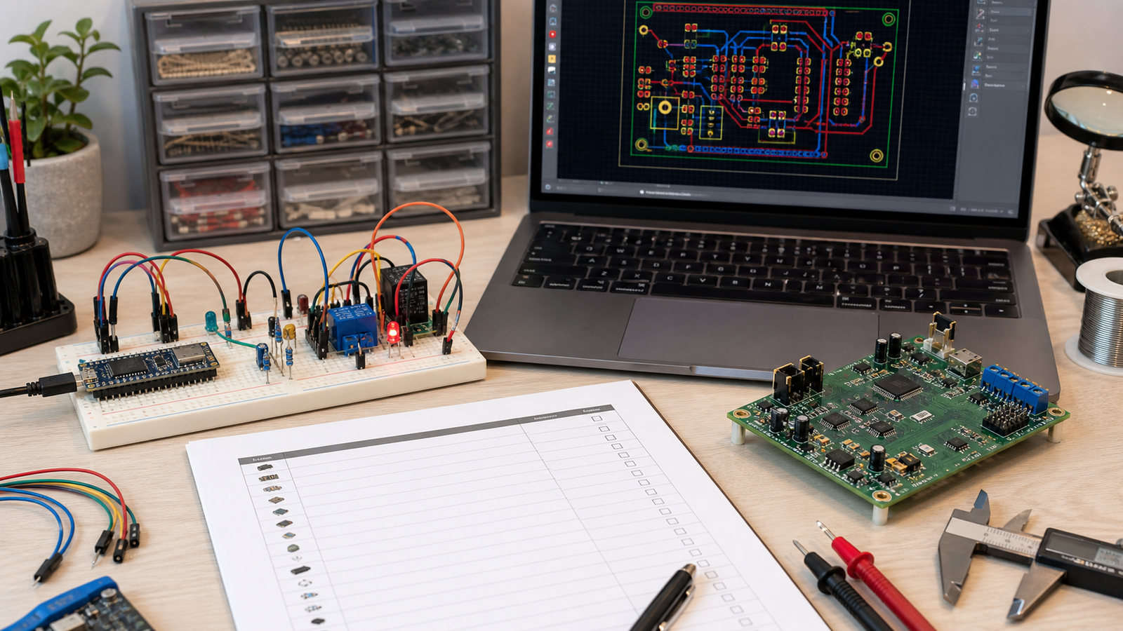
The full breadboard-to-PCB workflow
First-time PCB failures often happen because builders skip documentation and jump straight into layout. Slow down once, and the board spin becomes much cleaner.

PCB readiness scorecard
If any of these areas are vague, your board is not ready. Fix the uncertainty before spending money on fabrication.

Before designing the PCB: document the working circuit
- Draw the exact wiring used in the working prototype.
- Record every module pinout, power rail, ground connection, and signal name.
- Measure current draw in idle, active, Wi-Fi, relay switching, motor, or GSM transmit states.
- List exact modules and parts used, including seller links and part markings.
- Decide what will remain as a module and what will become bare components.
- Define connector names instead of vague jumper wires.
If you cannot redraw the breadboard circuit from your notes without looking at the breadboard, it is not ready for PCB layout.
PCB design checks
Power and grounding
- Use trace widths suitable for current.
- Add decoupling capacitors near IC/module power pins.
- Keep noisy loads away from sensitive analog or RF paths.
- Plan ground return paths instead of hoping copper fill fixes everything.
Connectors and labels
- Use keyed or clearly labeled connectors when polarity matters.
- Mark voltage, GND, pin 1, and orientation on silkscreen.
- Leave room for cable bending and enclosure access.
- Choose connector pitch that matches real wires and tools.
Test and programming
- Add test points for every power rail.
- Expose UART, I2C, reset, boot, and programming pins.
- Make test points reachable after assembly.
- Plan first-power-up current limiting and checks.
Mechanical
- Add mounting holes early, not at the end.
- Place buttons, LEDs, USB, displays, and connectors around enclosure needs.
- Check component height and keep-out areas.
- Confirm board outline before exporting Gerbers.
Manufacturing handoff checklist
| File or item | Needed for | What to check |
|---|---|---|
| Gerber files | PCB fabrication | All copper, solder mask, paste, silkscreen, and outline layers exported |
| Drill files | PCB fabrication | Plated and non-plated holes included and units correct |
| BOM | Assembly and sourcing | MPNs, values, footprints, quantity, package, alternates, and availability |
| Pick-and-place | Assembly | Reference designators, X/Y coordinates, rotation, and board side |
| Assembly notes | PCBA vendor or manual assembly | Do-not-populate parts, polarity, special handling, hand-soldered parts |
| Test plan | Bring-up | Power-up order, expected voltages, firmware flashing, basic functional tests |
Common first-PCB mistakes
- No programming header or boot/reset access.
- No test points for power rails.
- Wrong connector orientation or unlabeled connector pins.
- Footprint chosen by name without checking dimensions against the actual part.
- Assuming breadboard module wiring can be copied directly to a bare IC design.
- No mounting holes or enclosure clearance.
- Missing pullups, decoupling capacitors, level shifting, or protection components.
- Ordering assembly before BOM and footprint orientation are reviewed.
Modules vs bare ICs on the first PCB
It is okay to use modules on a first PCB. ESP32 modules, OLED modules, buck converters, or sensor modules can reduce risk. Move to bare ICs when size, cost, reliability, or production quantity justifies the extra design work.
Lower risk and faster validation.
Better cost, size, and control when you know the requirements.
Use modules for RF/power risk and bare parts for simple circuits.
FAQ
When is a breadboard project ready for PCB?
A project is ready when it works repeatedly, power needs are measured, connectors and test points are defined, the BOM is clear, and mechanical constraints are understood.
Should I design a PCB before the code is finished?
Only if hardware requirements are stable. If pin choices, sensors, power, or communication buses are still changing, wait or design in flexibility.
Should I use modules or bare ICs?
Use modules for the first PCB when they reduce RF, power, or assembly risk. Use bare ICs when you need lower cost, smaller size, or production control.
What files do I need for PCB assembly?
For assembly you usually need Gerbers, drill files, BOM, pick-and-place file, and assembly notes.
Want a second look before your first PCB order?
PCBVault can review your prototype-to-PCB plan, BOM, connector choices, test points, and manufacturing handoff risks.
See project review options